Atomically Thin Materials Significantly Shrink Qubits
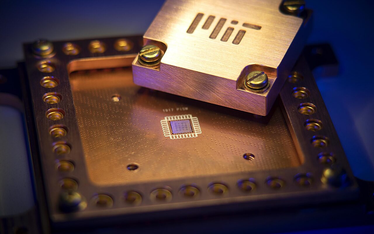

Quantum computing is a devilishly complex technology, with many technical hurdles impacting its development. Of these challenges two critical issues stand out: miniaturization and qubit quality.
IBM has adopted the superconducting qubit road map of reaching a 1,121-qubit processor by 2023, leading to the expectation that 1,000 qubits with today’s qubit form factor is feasible. However, current approaches will require very large chips (50 millimeters on a side, or larger) at the scale of small wafers, or the use of chiplets on multichip modules. While this approach will work, the aim is to attain a better path toward scalability.
Now researchers at MIT have been able to both reduce the size of the qubits and done so in a way that reduces the interference that occurs between neighboring qubits. The MIT researchers have increased the number of superconducting qubits that can be added onto a device by a factor of 100.
“We are addressing both qubit miniaturization and quality,” said William Oliver, the director for the Center for Quantum Engineering at MIT. “Unlike conventional transistor scaling, where only the number really matters, for qubits, large numbers are not sufficient, they must also be high-performance. Sacrificing performance for qubit number is not a useful trade in quantum computing. They must go hand in hand.”
The key to this big increase in qubit density and reduction of interference comes down to the use of two-dimensional materials, in particular the 2D insulator hexagonal boron nitride (hBN). The MIT researchers demonstrated that a few atomic monolayers of hBN can be stacked to form the insulator in the capacitors of a superconducting qubit.
Just like other capacitors, the capacitors in these superconducting circuits take the form of a sandwich in which an insulator material is sandwiched between two metal plates. The big difference for these capacitors is that the superconducting circuits can operate only at extremely low temperatures—less than 0.02 degrees above absolute zero (-273.15 °C).
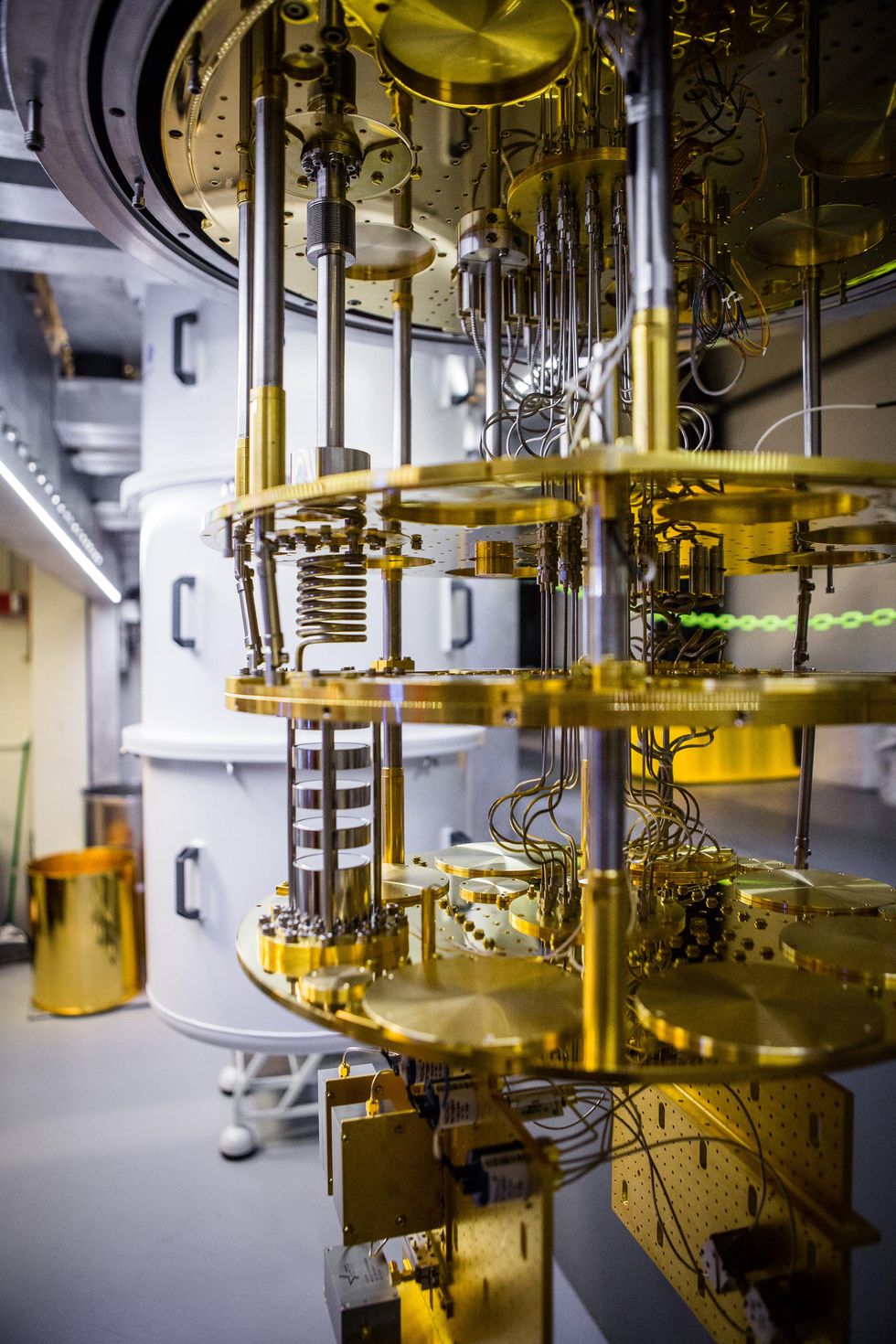
Superconducting qubits are measured at temperatures as low as 20 millikelvin in a dilution refrigerator.Nathan Fiske/MIT
In that environment, insulating materials that are available for the job, such as PE-CVD silicon oxide or silicon nitride, have quite a few defects that are too lossy for quantum computing applications. To get around these material shortcomings, most superconducting circuits use what are called coplanar capacitors. In these capacitors, the plates are positioned laterally to one another, rather than on top of one another.
As a result, the intrinsic silicon substrate below the plates and to a smaller degree the vacuum above the plates serve as the capacitor dielectric. Intrinsic silicon is chemically pure and therefore has few defects, and the large size dilutes the electric field at the plate interfaces, all of which leads to a low-loss capacitor. The lateral size of each plate in this open-face design ends up being quite large (typically 100 by 100 micrometers) in order to achieve the required capacitance.
In an effort to move away from the large lateral configuration, the MIT researchers embarked on a search for an insulator that has very few defects and is compatible with superconducting capacitor plates.
“We chose to study hBN because it is the most widely used insulator in 2D material research due to its cleanliness and chemical inertness,” said colead author Joel Wang, a research scientist in the Engineering Quantum Systems group of the MIT Research Laboratory for Electronics.
On either side of the hBN, the MIT researchers used the 2D superconducting material, niobium diselenide. One of the trickiest aspects of fabricating the capacitors was working with the niobium diselenide, which oxidizes in seconds when exposed to air, according to Wang. This necessitates that the assembly of the capacitor occur in a glove box filled with argon gas.
While this would seemingly complicate the scaling up of the production of these capacitors, Wang doesn’t regard this as a limiting factor.
“What determines the quality factor of the capacitor are the two interfaces between the two materials,” said Wang. “Once the sandwich is made, the two interfaces are “sealed” and we don’t see any noticeable degradation over time when exposed to the atmosphere.”
This lack of degradation is because around 90 percent of the electric field is contained within the sandwich structure, so the oxidation of the outer surface of the niobium diselenide does not play a significant role anymore. This ultimately makes the capacitor footprint much smaller, and it accounts for the reduction in cross talk between the neighboring qubits.
“The main challenge for scaling up the fabrication will be the wafer-scale growth of hBN and 2D superconductors like [niobium diselenide], and how one can do wafer-scale stacking of these films,” added Wang.
Wang believes that this research has shown 2D hBN to be a good insulator candidate for superconducting qubits. He says that the groundwork the MIT team has done will serve as a road map for using other hybrid 2D materials to build superconducting circuits.
المصدر: IEEE Spectrum